


We have a strong interest in exploring and designing devices such as: electronic, opto-electronic, sensors and actuators, photodetectors, solar cells, and quantum-scale devices. Besides forming such devices on conventional Si and crystalline substrates, we are also exploring transfer techniques to form such devices on flexible, transparent and conformable substrates.
Example of our recent work on high-performance MoS2 photodetectors
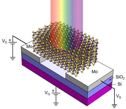
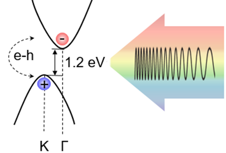
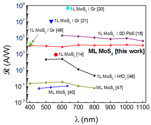
In our recent work that appeared in Nature Scientific Reports, we demonstrated ultra-high photoresponsivity in suspended metal-semiconductor-metal (MSM) MoS2 broadband photodetectors with low Schottky-barrier contacts. In the paper, we report on the design, fabrication, and characterization of ultra-high responsivity photodetectors based on mesoscopic multilayer MoS2, which is a less explored system compared to direct band gap monolayer MoS2 that has received increasing attention in recent years. The device architecture is comprised of a MSM photodetector, where Mo was used as the contact metal to suspended MoS2 membranes. The photoresponsivity R was measured to be ~ 1.4 x 10^4 A/W, which is >10,000 times higher compared to prior reports, while the detectivity D* was computed to be ~ 2.3 x 10^11 Jones at 300 K at an optical power P of ~ 14.5 pW and wavelength λ of ~ 700 nm. In addition, the dominant photocurrent mechanism was determined to be the photoconductive effect (PCE), while a contribution from the photogating effect was also noted from trap-states that yielded a wide spectral photoresponse from UV-to-IR (400 nm to 1100 nm) with an external quantum efficiency (EQE) ~ 10^4. From time-resolved photocurrent measurements, a decay time of ~ 2.5 ms was measured at 300 K from the falling edge of the photogenerated waveform after irradiating the device with a stream of incoming ON/OFF white light pulses. For more details on this work, we refer you to our recently published MoS2 photodetector article.
Besides our efforts in MoS2-based devices, we are also interested in forming high-performance opto-electronic devices, including solar cells, using WSe2, WS2, perovskites and black phosphorus.
We use a cryogenic probe stage that allows us to conduct electronic and optoelectronic measurements of devices at low temperatures and in vacuum environments. Coupled to this cryogenic probe stage, we also have ultra low-noise electronic instrumentation for measuring the electronic transport properties of our materials and devices. We also have the ability to irradiate the device under test using tunable laser sources from the visible to the NIR regime and measure the optoelectronic response of the devices as a function of temperature.
Lakeshore Cryogenic Probe Stage
